
How Are PCBs Made Step by Step?

Image Source: depositphotos.com
The PCB manufacturing process is a fascinating blend of electrical engineering, materials science, and high-tech craftsmanship,whether you're designer, hobbyist, or industry executive, you should understanding how printed circuit boards (PCBs) are made equip you to create better projects, solve problem, and collaborate more effectively with manufacturing partner.
In this deep-dive, we will walk you through the entire pcb fabrication process—from design PCB and pcb printing to the last step of the process involving optical inspection and test. We will step-by-step guide uncovers each key stage of production, explain how complex circuit are realize from scratch, and highlight why sharp-eyed inspector give each PCB the final check before delivery.
What Are PCBs and How Do They Work?
The printed circuit board (PCB) is the backbone of every electronic device,often called the heart or nervous system of modern technology, PCBs mechanically support and electrically connect component using copper foil trace in designed pattern, each copper path acts as a highway for electrical signal, enabling your phone, laptop, or IoT sensor to work seamlessly.
There are several type of PCBs, include single-sided PCB, two-layer PCB, and multilayer PCB architecture, the variety is vast because every device has its own PCB needs — from the simple circuits in a TV remote to the complex process of constructing the main board for an autonomous vehicle.
A Brief History: The Evolution of Circuit Board Manufacturing
The journey of printed circuit board manufacturing began in the early 20th century, which revolutionizing electronics, ago boards were laboriously hand-wired, but mass production demanded efficient alternative, in the 1940s the subtracting process where unwanted copper was etched away from large copper sheets emerged — still core to today's industry.
The advent of Gerber files (the standard for PCB design output) and PCB design software in 1970s made production both precise and repeatable. Since then the advancement such as HDI (High-Density Interconnect) boards, surface finish innovation (like Electroless Nickel Immersion Gold), and fine-pitch multilayer PCBs have kept pushing electronics forward.
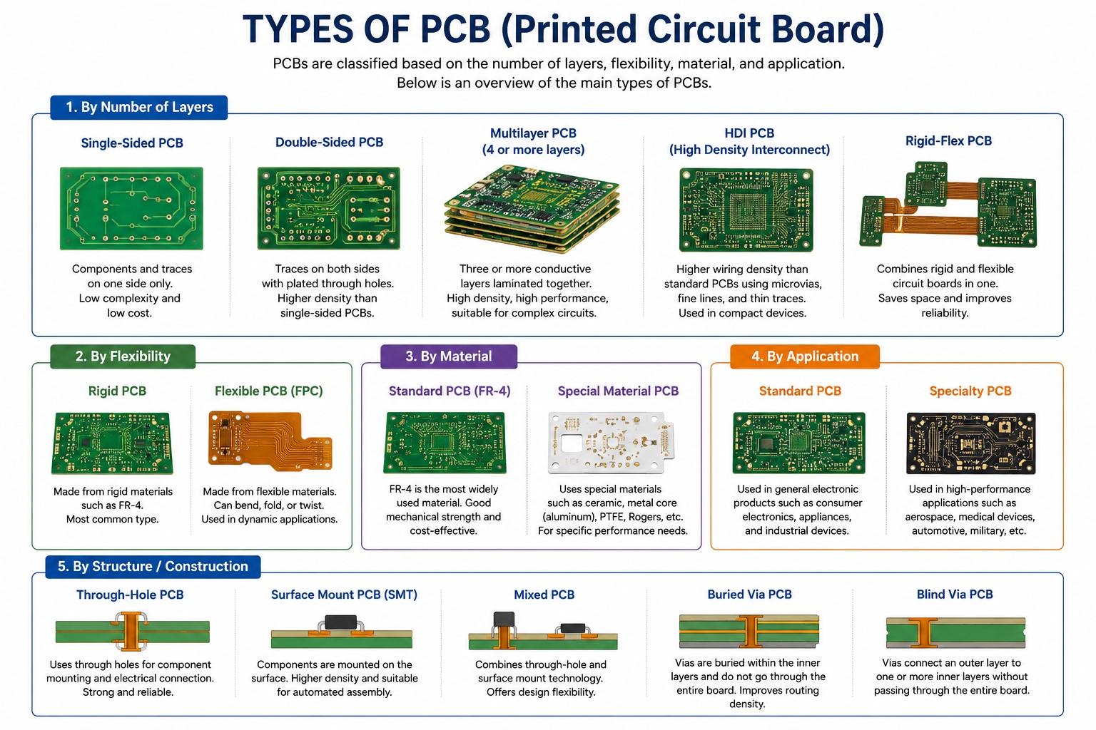
Types of PCBs and Their Applications
PCBs come in many forms, depending on device requirements. Consider these key types:
|
PCB Type |
Description |
Typical Use Cases |
|
Single-sided |
One copper layer on an insulating substrate |
Basic toys, calculators |
|
Two-layer PCB |
Copper layers on both sides of the board |
Power supplies, larger appliances |
|
Multilayer PCB |
Multiple inner and outer layers, often up to 30+ |
Servers, smartphones, aerospace |
|
Rigid |
Standard hard FR-4-based boards |
Computers, industrial equipment |
|
Flex/Flex-Rigid |
Polyimide-based flexible or hybrid structures |
Wearables, foldable devices |
|
HDI |
High-density interconnect, microvias and thin traces |
Mobile, SSDs, high-speed circuits |
Anatomy of a PCB: Key Parts and Layers
To truly understand how circuit board are manufactured, it’s essential to know the part of the PCB and the function of each layer of the board:
- Substrate (Laminate Board/FR-4/Polyimide/Rogers): The structure and insulator of the board, supporting the rest of the stack.
- Copper Foil: Thin copper foil is laminated to the substrate to form the initial conductive surface,all traces and pad are created by removing unwanted copper during etching. Both inner and outer copper layers exist in a multi-layer PCB.
- Prepreg: Layers that bond multiple copper foils in a laminating process
- Solder Mask: Applied to the outer layer (and sometime to inner layers of rigid-flex designs) to protect the copper from oxidation and prevent solder bridging.
- Silkscreen: Add marking and part IDs to the board, making assembly and troubleshooting easier
- Vias and Through Holes: Conductive connections between sides of the board or across multiple PCB layers, created during the drilling process.
A two-layer PCB need four phototool (top copper, bottom copper, top solder mask, bottom solder mask),a complex ten-layer PCB will have many more, each one correspond to specific layers of the PCB.
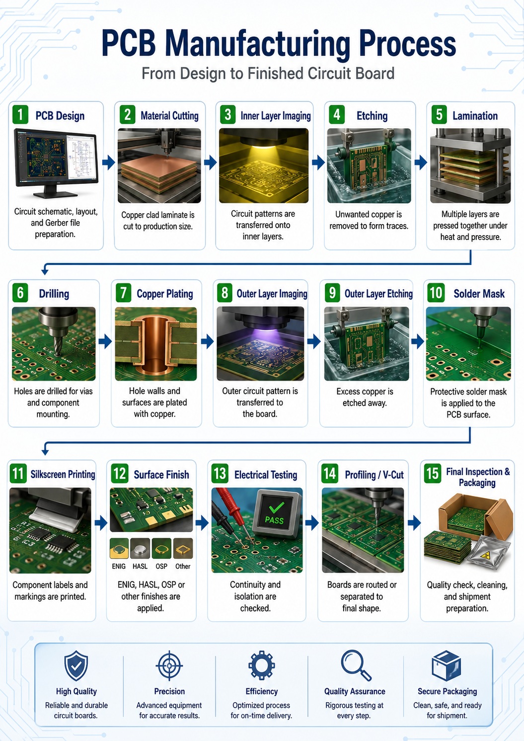
The PCB Manufacturing Process: A Step-by-Step Guide
Let’s explore each stage of the pcb fabrication process in detail, each step in the manufacturing process is critical for consistency, performance, and yield:
1. PCB Design and Printing Begins
The design process start in pcb design software, the engineers create a schematic, and then layout the physical circuit — specifying exact trace, pad shape, and stack-up,once finalized:
- Gerber files are exported, representing every layer of the pcb;
- For every board, drill file, overlay (silkscreen), and a bill of material complete the actual PCB documentation
- The pcb design is printed as a photo negative of the PCB (or directly image on photoresist in advanced fab line).
2. Phototooling and Imaging
In the classic approach, the production process begins with producing a film of the pcb (phototool) for each layer. In HDI board, digital direct imaging is increasingly common.
- The film is align to the PCB panel, it may include multiple copies of the board (efficient for volume production)
- The first thing of the imaging process applies a photosensitive layer (photoresist) to the copper.
- The film is overlaid, and UV light harden the exposed region, defining where copper will remain
3. Inner Layer Processing
For multi-layer pcb or multilayer PCB, the inner layers need processed first.
- Photoresist-covered inner layers are imaged and develop, leaving protected and uncovered regions
- In the next thing of manufacturing processes, the boards are sent through the chemical etching process:
- Etch away the unwanted copper; only the intend trace remain on each inner layer.
- After etching, AOI inspectors give each PCB an optical inspection, every board is compared against the original board design data to ensuring no shorts, opens, or misconnections.
4. Layer Stack-Up and Laminating Process
All layers are aligned with registration holes, “stacked up,” and fused with prepreg using heat and pressure in a laminating process.
- The thin layer of copper for the outermost (top and bottom) layers is added during this step.
- Larger volume lines use CNC-controlled presses and punch machines to ensure its repeatability.
For multilayer PCB the laminating process is the magic happens: multiple inner layers, each patterned with copper traces, are sandwiched with insulating prepreg and topped with a thin copper foil to form the outer layers of the PCB, the stack is heat and press under high pressure in a hydraulic press. This bonds all layers into a single, robust board.
- Registration holes and alignment pin ensure that each layer of the board is perfectly aligned, it is crucial for complex, high-density circuits even a tiny alignment issue can cause malfunction.
- The process involve a collaboration between automation, as misalignment at this stage could lead to costly rework or scrapping.
5. Drilling Process: Creating Holes and Vias
Then the holes are drilled using high-precision CNC machines. This step forms vias (to connect different pcb layers) and mounting holes for component.
- The drill sequence is programmed from the designer’s file, and hole as small as 0.1mm can be achieve for advance design.
- For densely-packed boards, “blind,” “buried,” and “micro-vias” connect only select layers rather than run through the entire stack—essential for HDI and advanced multilayer circuit.
- After drilling the desmearing with chemical bath removes any residue, and ready the holes for plating.
6. Plating Process: Metalizing the Holes
The plating process gives conductivity to drilled holes:
- First, an electroless copper bath coats a thin layer of copper inside every drilled hole. This “seeds” the surface for the next step.
- The board is then submerged in an electrolytic copper plating tank. This is the first step in the plating process that builds up the copper further.
- Additional plating steps may deposit nickel, gold, or tin, depending on the circuit board’s use and the surface finish specified.
7. Imaging and Etching the Outer Layers
- The outer layers of the PCB now have copper foil, which, like the inner layers, is patterned by applying photoresist, exposing with UV light against a fresh phototool (the step of the imaging process), then developing.
- The place not protected by photoresist or film will undergo a chemical etching process to etch away the unwanted coppers, then the final circuit on the finished PCB.
8. Solder Mask and Silkscreen Application
Then the solder mask is applied for the next. This thin layer is usually green and also can be other colors such as red, blue, or black for branding or visual clarity.
- The solder mask protect copper trace from oxidation, and prevents solder bridges, and mechanically insulates the board’s surface.
- The mask is precisely patterned to expose only pads and vias that will receive solder—a critical step for SMT (surface mount) circuit.
Following solder mask application, the silkscreen layer(legend) is printed. This adds part number, logos, and alignment marks to the outer layer, the aid the pcb assembly team and future repair.
9. Surface Finish: Enhancing Solderability and Longevity
Now exposed copper pads and vias are treated with a surface finish. Different pcb application demand different finish treatment, but some common options are:
|
Surface Finish |
Description |
Best Use |
|
HASL (Hot Air Solder Level) |
Molten solder layer and leveled by hot air knives |
General purpose |
|
ENIG (Electroless Nickel Immersion Gold) |
Flat and durable nickel/gold layer |
BGAs, fine-pitch SMT |
|
OSP (Organic Solderability Preservative) |
Thin organic film |
Short-use consumer goods |
|
Immersion Silver/Gold |
Flat and low-resistance finish for RF/high-reliability |
High-frequency, RF boards |
- The production process and end-use environment determine the best finish for a given job.
- Electroless nickel immersion gold is often chosen for its excellent shelf life, solderability, and flatness—ideal for fine-pitch and ball grid array (BGA) packages.
10. Final Steps: Routing, Scoring, and Profile Cutting
When the circuitry is complete the board are routed out of the pcb panel using a CNC machine, or scored with V-cut for easy separation (sometimes performed by a punch machine for simple outlines).
- This “singulation” process turns a panel of many units into individual boards.
- Panel reduce cost and increase throughput during the earlier manufacture process, but for delivery to customer or pcb assembly, the final finish PCB must be cut, clean, and pack.
11. Inspection, Testing, and Quality Control
The latest thing of the process is stringent inspection and functional testing:
- Automated Optical Inspection (AOI): Camera compare the board’s trace, width, and feature to the digital design, catching missing or extra copper, nick, and bridging.
- Electrical Tests on the PCB: Flying probe, bed-of-nail, or netlist comparison systems are use to ensure every net is continuous and there are no short.
- FQC give each pcb a final check—looking for cosmetic issues, Foreign Object Debris (FOD), or solder mask misalignment.
Quality Note: In medical, aerospace, or automotive sectors, microsectioning (cross-sectional analysis), ionic contamination tests, and enhanced reliability verification are often required.
PCB Assembly and Board Delivery
After printed circuit board manufacturing and the complete board manufacturing process, bare boards move to the pcb assembly stage:
- SMT (Surface Mount Technology) and THT (Through-Hole Technology) are used to attach components.
- Assembly yield depends on final PCB quality, flatness (for accurate pick-and-place component placement), and surface finish.
- Finish PCB boards undergo final round of electrical, functional, and sometime environmental testing before being packaged and usually in moisture barrier bags with desiccants and ESD-safe package for delivery.
Environmental and Compliance Factors in the PCB Industry
- The PCB industry is rapid evolving toward greener process. This includes RoHS and REACH compliance (lead-free, low-halogen materials), closed-loop chemical systems, copper recycling from etchant, and water reduction.
- Green solder masks, recyclable substrate, and efficient energy use in pcb manufacture are becoming a competitive advantage as global customers demand traceable, sustainable hardware.
Common Questions and Troubleshooting
Q: Why does my board have missing copper or thin traces?
A: Issues during the chemical etching process or inadequate photoresist exposure can etch away desired copper. Always check for even exposure and proper etchant refresh.
Q: What is the difference between HASL and ENIG surface finishes?
A: HASL is cost-effective but not perfectly flat. ENIG—or Electroless Nickel Immersion Gold—provides a smooth, durable surface, ideal for fine-pitch components and high-reliability needs.
Q: Can the PCB design affect the reliability of the final assembly?
A: Absolutely. Unclear or overlapping layers, poor pad design, or lack of DFM review can cause failures in the finished product, making the design process and manufacturing review essential.
Q: Why is solder mask alignment so important?
A: Poor solder mask alignment can expose traces to oxidation or cause accidental shorts during assembly.
Q: How do I choose the right number of layers for my PCB?
A: Consider signal complexity, EMI requirements, mechanical strength, and available space. Multilayer circuits support EMI shielding and power integrity in high-speed/high-density designs.
Conclusion: The Future of PCB Manufacturing
The world of printed circuit board manufacturing is more dynamic and demanding than ever. Modern PCB fabrication is a complex process—each step in the manufacturing process is interacting with other things. The shift to smaller, faster, and more reliable electronics is driving innovations in everything from board manufacturing process steps (additive manufacturing, embedded components) to the use of new materials like ceramics or hybrid laminates.
By following best practices and understanding the complete PCB journey—from initial pcb design is printed through final inspection and assembly—you help make a PCB that meets today’s high expectations.